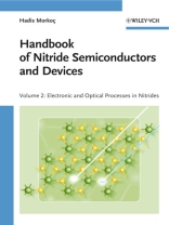
The three volumes of this handbook treat the fundamentals, technology and nanotechnology of nitride semiconductors with an extraordinary clarity and depth. They present all the necessary basics of semiconductor and device physics and engineering together with an extensive reference section. The handbook also deals with the properties and processes for thermal, optical (3-, 2-, 1-, 0-dimensional systems), electrical (at low- and high-electric fields, low- and high-magnetic fields for 3- and 2-dimensional systems), magnetism and magnetic properties (in dilute magnetic ion doped compounds) and spin-based device concepts. Volume 2 deals with the electrical and optical properties of nitride materials.
Зміст
1 Metal Contacts to Ga N and Processing
1.1 A Primer for Semiconductor-Metal Contacts
1.2 Current Flow in Metal-Semiconductor Junctions
1.3 Ga N Schottky Barriers for High-Voltage Rectifiers
1.4 Ohmic Contact Resistance
1.5 Determination of the Contact Resistivity
1.6 Ohmic Contacts to Ga N
1.7 Structural Analysis of Ohmic Contacts on Ga N
1.8 Etching Techniques for III Nitrides
1.9 Implant Isolation
1.10 Process Damage
2 Determination of Impurity and Carrier Concentrations
2.1 Impurity Binding Energy
2.2 Conductivity Type: Hot Probe and Hall Measurements
2.3 Semiconductor Statistics, Density of States, and Carrier Concentration
2.4 Capacitance-Voltage Measurements
3 Carrier Transport
3.1 Prelude
3.2 Carrier Scattering
3.3 Calculated Mobility of Ga N
3.4 Scattering at High Fields
3.5 Measurements of Mobility and Associated Fundamentals
3.6 Multiband Effects and Mixed Conductivity
3.7 van der Pauw Method
3.8 Quantum Hall Effect – Shubnikov-de Haas
3.9 Measured Mobility in n-type Ga N
3.10 Measurement of High-Field Electron Velocity in n-Type Ga N
3.11 Carrier Transport in p-Type Ga N
3.12 Carrier Transport in In N
3.13 Carrier Transport in Al N
3.14 Transport in Unintentionally Doped and High-Resistivity Ga N
3.15 Carrier Transport in Alloys
3.16 Two-Dimensional Transport in n-Type Ga N
3.17 Interface Roughness Scattering
3.18 Quantum Transport in Al Ga N/Ga N 2DEG
3.19 Observations
4 The p-n Junction
4.1 Heterojunctions
4.2 Band Discontinuities
4.3 Electrostatic Characteristics of p-n Heterojunctions
4.4 Current-Voltage Characteristics of p-n Junctions
4.5 I-V Characteristics of Ideal Ga N-Based p-n Junctions
4.6 I-V Characteristics of Ga N-Based p-n Junctions
4.7 High-Voltage Blocking Ga N and Al Ga N-Based p-n Junctions
5 Optical Processes in Semiconductors and Optical Properties of Nitride Semiconductors and Heterostructures
5.1 Basics of Photoluminescence
5.2 Band-to-Band Transitions
5.3 Optical Transitions in Ga N
5.4 Group-II Element Related Transitions
5.5 Blue Luminescence Band in Undoped Ga N
5.6 Surface-Related Blue Luminescence in Etched Ga N
5.7 Optical Properties of Ga N Doped with Rare Earths
5.8 Optical Properties of Alloys
5.9 Optical Properties of Nitride Heterostructures
5.10 Quantum Dots
5.11 Intraband or Intersubband Transitions in Ga N/Al Ga N Quantum Wells
5.12 Nonlinear Optical Properties of III-Nitrides
Про автора
Hadis Morkoç received his Ph.D. degree in Electrical Engineering from Cornell University. From 1978 to 1997 he was with the University of Illinois, then joined the newly established School of Engineering at the Virginia Commonwealth University in Richmond. He and his group have been responsible for a number of advancements in Ga N and devices based on them. Professor Morkoç has authored several books and numerous book chapters and articles. He serves or has served as a consultant to some 20 major industrial laboratories. Professor Morkoç is, among others, a Fellow of the American Physical Society, the Material Research Society, and of the Optical Society of America.


