Chemical Mechanical Planarization (CMP) plays an important role in today’s microelectronics industry. With its ability to achieve global planarization, its universality (material insensitivity), its applicability to multimaterial surfaces, and its relative cost-effectiveness, CMP is the ideal planarizing medium for the interlayered dielectrics and metal films used in silicon integrated circuit fabrication. But although the past decade has seen unprecedented research and development into CMP, there has been no single-source reference to this rapidly emerging technology-until now.
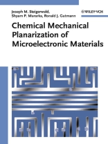
Chemical Mechanical Planarization of Microelectronic Materials provides engineers and scientists working in the microelectronics industry with unified coverage of both the fundamental mechanisms and engineering applications of CMP. Authors Steigerwald, Murarka, and Gutmann-all leading CMP pioneers-provide a historical overview of CMP, explain the various chemical and mechanical concepts involved, describe CMP materials and processes, review the latest scientific data on CMP worldwide, and offer examples of its uses in the microelectronics industry. They provide detailed coverage of the CMP of various materials used in the making of microcircuitry: tungsten, aluminum, copper, polysilicon, and various dielectric materials, including polymers. The concluding chapter describes post-CMP cleaning techniques, and most chapters feature problem sets to assist readers in developing a more practical understanding of CMP.
The only comprehensive reference to one of the fastest growing integrated circuit manufacturing technologies, Chemical Mechanical Planarization of Microelectronic Materials is an important resource for research scientists and engineers working in the microelectronics industry.
An indispensable resource for scientists and engineers working in the microelectronics industry
Chemical Mechanical Planarization of Microelectronic Materials is the only comprehensive single-source reference to one of the fastest growing integrated circuit manufacturing technologies. It provides engineers and scientists who work in the microelectronics industry with unified coverage of both the fundamental mechanisms and engineering applications of CMP, including:
* The history of CMP
* Chemical and mechanical underpinnings of CMP
* CMP materials and processes
* Applications of CMP in the microelectronics industry
* The CMP of tungsten, aluminum, copper, polysilicon, and various dielectrics, including polymers used in integrated circuit fabrication
* Post-CMP cleaning techniques
* Chapter-end problem sets are also included to assist readers in developing a practical understanding of CMP.
Table des matières
Chemical Mechanical Planarization-An Introduction.
Historical Motivations for CMP.
CMP Variables and Manipulations.
Mechanical and Electrochemical Concepts for CMP.
Oxide CMP Process-Mechanisms and Models.
Tungsten and CMP Processes.
Copper CMP.
CMP of Other Materials and New CMP Applications.
Post-CMP Cleanup.
Appendix.
Index.
A propos de l’auteur
JOSEPH M. STEIGERWALD, Ph D, works for the Intel Corporation in Hillsboro, Oregon. Currently developing CMP processes for dielectric films, he has also worked for Intel in the areas of plasma and wet etching of thin films. Dr. Steigerwald earned his Ph D at Rensselaer Polytechnic Institute, where his thesis involved fundamental aspects of copper CMP. He holds a bachelor’s degree in electrical engineering from Clarkson University.
SHYAM P. MURARKA, Ph D, is Director of the SRC Center for Advanced Interconnect Science and Technology at Rensselaer Polytechnic Institute, and a professor with the Center for Integrated Electronics and Electronics Manufacturing (CIEEM) and the Materials Science and Engineering Department at Rensselaer. He has also served as the Director of CIEEM (1994-1996) and Co-Director of New York’s SEMATECH Center of Excellence in Multilevel Interconnects (1990-1996). He is a Fellow of ASM International, IEEE, and AVS, and a member of the Electrochemical Society, TMS, and MRS. Dr. Murarka received a doctorate in chemistry from Agra University in India and one in metallurgy and materials science from the University of Minnesota.
RONALD J. GUTMANN, Ph D, is Professor in Rensselaer Polytechnic Institute’s Department of Electrical, Computer and Systems Engineering, Coordinator of multifaculty programs in Low Dielectric Constant Interconnect Technology and Thermophotovoltaic Cell Technology, and a member of both the SEMATECH University Advisory Council and the Semiconductor Research Corporation University Advisory Committee. From 1989 to 1994 he served as Director of the Rensselaer Center for Integrated Electronics, an interdisciplinary research and education center involving 50 faculty with programs in electronic materials, processing techniques, semiconductor devices, characterization techniques, and VLSI design, and from 1990 to 1996 as Co-Director of New York’s Sematech Center of Excellence in Multilevel Interconnects. He is a Fellow of ieee. Dr. Gutmann received both his bachelor of electrical engineering degree and doctorate in electrophysics from Rensselaer Polytechnic Institute.
