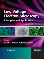
Part of the Wiley-Royal Microscopical Society Series, this book discusses the rapidly developing cutting-edge field of low-voltage microscopy, a field that has only recently emerged due to the rapid developments in the electron optics design and image processing.
It serves as a guide for current and new microscopists and materials scientists who are active in the field of nanotechnology, and presents applications in nanotechnology and research of surface-related phenomena, allowing researches to observe materials as never before.
Daftar Isi
List of Contributors ix
Preface xi
1 Introduction to the Theory and Advantages of Low Voltage Electron Microscopy 1
David C. Bell and Natasha Erdman
1.1 Introduction 1
1.2 Historical Perspective 2
1.3 Beam Interaction with Specimen–Elastic and Inelastic Scattering 3
1.4 Instrument Configuration 11
1.5 Influence of Electron Optics Aberrations at Low Voltages12
1.6 SEM Imaging at Low Voltages 16
1.7 TEM/STEM Imaging and Analysis at Low Voltages 26
1.8 Conclusion 27
References 28
2 SEM Instrumentation Developments for Low k V Imaging and Microanalysis 31
Natasha Erdman and David C. Bell
2.1 Introduction 31
2.2 The Electron Source 33
2.3 SEM Column Design Considerations 36
2.4 Beam Deceleration 41
2.5 Novel Detector Options and Energy Filters 43
2.6 Low Voltage STEM in SEM 48
2.7 Aberration Correction in SEM 50
2.8 Conclusions 53
References 53
3 Extreme High-Resolution (XHR) SEM Using a Beam Monochromator 57
Richard J. Young, Gerard N.A. van Veen, Alexander Henstraand Lubomir Tuma
3.1 Introduction 57
3.2 Limitations in Low Voltage SEM Performance 58
3.3 Beam Monochromator Design and Implementation 59
3.4 XHR Systems and Applications 63
3.5 Conclusions 69
Acknowledgements 70
References 70
4 The Application of Low-Voltage SEM–From Nanotechnology to Biological Research 73
Natasha Erdman and David C. Bell
4.1 Introduction 73
4.2 Specimen Preparation Considerations 74
4.3 Nanomaterials Applications 76
4.4 Beam Sensitive Materials 84
4.5 Semiconductor Materials 85
4.6 Biological Specimens 87
4.7 Low-Voltage Microanalysis 91
4.8 Conclusions 92
References 93
5 Low Voltage High-Resolution Transmission Electron Microscopy 97
David C. Bell
5.1 Introduction 97
5.2 So How Low is Low? 99
5.3 The Effect of Chromatic Aberration and Chromatic Aberration Correction 100
5.4 The Electron Monochromator 103
5.5 Theoretical Tradeoffs of Low k V Imaging 105
5.6 Our Experience at 40 ke V LV-HREM 109
5.7 Examples of LV-HREM Imaging 110
5.8 Conclusions 114
References 116
6 Gentle STEM of Single Atoms: Low ke V Imaging and Analysisat Ultimate Detection Limits 119
Ondrej L. Krivanek, Wu Zhou, Matthew F. Chisholm, Juan Carlos Idrobo, Tracy C. Lovejoy, Quentin M. Ramasse and Niklas Dellby
6.1 Introduction 119
6.2 Optimizing STEM Resolution and Probe Current at Low Primary Energies 121
6.3 STEM Image Formation 128
6.4 Gentle STEM Applications 135
6.5 Discussion 154
6.6 Conclusion 156
Acknowledgements 157
References 157
7 Low Voltage Scanning Transmission Electron Microscopy of Oxide Interfaces 163
Robert Klie
7.1 Introduction 163
7.2 Methods and Instrumentation 166
7.3 Low Voltage Imaging and Spectroscopy 168
7.4 Summary 180
Acknowledgements 180
References 180
8 What’s Next? The Future Directions in Low Voltage Electron Microscopy 185
David C. Bell and Natasha Erdman
8.1 Introduction 185
8.2 Unique Low Voltage SEM and TEM Instruments 186
8.3 Cameras, Detectors, and Other Accessories 192
8.4 Conclusions 198
References 199
Index 201
Tentang Penulis
David C. Bell received his Ph D in physics from the University of Melbourne, Australia in 1997 and completed his postdoctoral studies at MIT in 1999. He was research faculty and principal investigator at the University of Minnesota from 2000 to 2002. In 2003, he joined the Center for Nanoscale Systems at Harvard University as a principal scientist and became the Manager for Imaging and Analysis in 2007. He has been a lecturer in applied physics at Harvard since 2003 and is a teaching professor at the Harvard Extension School. In 2007, he was a visiting scientist at the Department of Materials, Oxford University, UK. Dr Bell is one of the renowned experts in the field of elemental analysis using electron microscopy (TEM and STEM) and has co-authored a book on this subject. He has authored more than 70 research papers on the subjects of microscopy, materials science and biology and holds several patents. He is an elected Fellow of the Royal Microscopical Society, UK.
Natasha Erdman received her Ph.D. in Materials Science and Engineering from Northwestern University (Chicago, IL) in 2002. After completing her Ph.D. she worked as a Senior Research Chemist at UOP LLC (currently Honeywell) in Des Plaines, IL focusing on investigation of structure-properties relationship in various catalysts using electron microscopy techniques. In 2004 Dr. Erdman as joined JEOL USA Inc., and currently serves as an SEM and Ion-Beam Product Manager. She has authored over 30 peer-reviewed papers on the subjects of microscopy, materials science, chemistry and biology and is a renowned expert on ion-beam based sample preparation techniques for electron microscopy.
