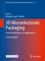
This book offers a comprehensive reference guide for graduate students and professionals in both academia and industry, covering the fundamentals, architecture, processing details, and applications of 3D microelectronic packaging. It provides readers an in-depth understanding of the latest research and development findings regarding this key industry trend, including TSV, die processing, micro-bumps for LMI and MMI, direct bonding and advanced materials, as well as quality, reliability, fault isolation, and failure analysis for 3D microelectronic packages. Images, tables, and didactic schematics are used to illustrate and elaborate on the concepts discussed. Readers will gain a general grasp of 3D packaging, quality and reliability concerns, and common causes of failure, and will be introduced to developing areas and remaining gaps in 3D packaging that can help inspire future research and development.
Daftar Isi
1. Introduction to 3D microelectronic packaging.- 2. 3D packaging architecture and assembly process design.- 3. Fundamentals of TSV processing and reliability.- 4. Mechanical properties of TSV.- 5. Atomistic View of TSV Protrusion/Intrusion.- 6. Fundamentals and failures in Die preparation for 3D packaging.- 7. Direct Cu to Cu bonding and other alternative interconnects in 3D packaging.- 8. Emerging hybrid bonding techniques for 3D packaging.- 9. Fundamental of Thermal Compressive Bonding process, advanced epoxy, and flux materials in 3D packaging.- 10. Fundamentals of solder alloys in 3D packaging.- 11. Fundamentals of electro migration in interconnects of 3D packages.- 12. Fundamentals of heat dissipation in 3D packaging.- 13. Fundamentals of advanced materials and process in substrate technology.- 14. New substrate technologies for 3D packaging. -15. Thermal mechanical and moisture modeling in 3D packaging.- 16. Stress and Strain measurements in 3D packaging.- 17.Processing and Reliability of Solder Interconnections in Stacked Packaging.- 18. Interconnect Quality and Reliability of 3D Packaging.- 19. Fundamentals of automotive reliability of 3D packages.- 20. Fault isolation and failure analysis of 3D packaging.
Tentang Penulis
Dr. Yan Li is currently a senior staff package engineer in Assembly Test and Technology Development Failure Analysis Lab of Intel Corporation located in Chandler, Arizona. Dr. Li received her Ph.D. degree in Materials Science and Engineering from Northwestern University in 2006, and her M.S and B.S degree in Physics from Peking University. As the lead package failure analysis engineer of 3D package technology development projects in Intel, Dr. Li has been actively involved in numerous packaging related technical solutions, and focusing on the quality and reliability of electronic packages, fundamental understanding of failure modes and failure mechanisms of electronic packages, developing new tools and techniques for fault isolation and failure analysis of 3D electronic packages. Dr. Li is a senior member and contributor of many international professional associations, such as Minerals Metals and Materials Society (TMS), American Society for Metals (ASM), and Electronic Device Failure Analysis Society (EDFAS). She has been appointed as TMS and International Symposium for Testing and Failure Analysis (ISTFA) annual conference organizer since 2011. Dr. Li joined the technical committee of International Symposium on the Physical and Failure Analysis of Integrated Circuits. (IPFA) since 2018. She was granted the TMS EMPMD Young Leader Professional Development Award in 2014. Dr. Li has published over 20 papers and two patents in the microelectronic packaging area. She is the co-editor of a semiconductor industry highly recognized book: “3D Microelectronic Packaging: From Fundamentals to Applications” by Springer.
Dr. Deepak Goyal is currently the Director of the ATTD/ATM Package FA & LYA Labs at Intel. Dr. Goyal graduated with a Ph D in Materials Science and Engineering from State University of New York, Stony Brook. His responsibilities include development of the next generation of analytical tools and techniques, defect characterization, fault isolation, failure and materials analyses for the next generation package, substrates and boards technology development at Intel and Package FA/LYA for Intel’s Assembly Test and Manufacturing. He has helped with the development of all Intel assembly technologies including FCx GA, FCCSP, TSVs, EMIB and Foveros. He is an expert in the failure analysis of packages and has taught Professional Development courses on Package FA/FI methods and failure mechanisms at the Electronics Components and Technology Conference (ECTC). He has won two Intel Achievement Awards and 25 Division Recognition Awards at Intel. Deepak has authored and co-authored over 50 papers and holds 11 US patents with 5 more in flight. He has co-authored several book chapters and has co-edited a book titled “3D Microelectronic Packaging – From Fundamentals to Applications”. He is a senior member of the IEEE and was the chair of the Package and Interconnect Failure Analysis Forum sponsored by the International Sematech and a past chair of the ECTC Applied Reliability Committee.


