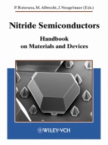
Semiconductor components based on silicon have been used in a wide range of applications for some time now. These elemental semiconductors are now well researched and technologically well developed. In the meantime the focus has switched to a new group of materials: ceramic semiconductors based on nitrides are currently the subject of research due to their optical and electronic characteristics. They open up new industrial possibilities in the field of photosensors, as light sources or as electronic components.
This collection of review articles provides a systematic and in-depth overview of the topic, on both a high and current level. It offers information on the physical basics as well as the latest results in a compact yet comprehensive manner. The contributions cover the physical processes involved in manufacture, from semiconductor growth, via their atomic structures and the related characteristics right up to future industrial applications. A highly pertinent book for anyone working in applied materials research or the semiconductor industry.
Tabella dei contenuti
1. High Pressure Crystallization of Ga N (I. Grzegory, S. Krukowski, M. Leszczynski, P. Perlin, T. Suski, and S. Porowski)
2. Epitaxial Lateral Overgrowth of Ga N (P. Gibart, B. Beaumont, and P. Vennéguès)
3. Plasma Assisted Molecular Beam Epitaxy of III-V Nitrides (A. Georgakilas, H. M. Ng, and Ph. Komninou)
4. The Growth of Gallium Nitride by Hydride Vapour Phase Epitaxy (HVPE) (A. Trassoudaine, R. Cadoret and E. Aujol)
5. Growth and Properties of In N (V. Yu. Davydov, A. A. Klochikhin, S. V. Ivanov, I. Aderhold, and A. Yamamoto)
6. Ab initio Analysis of Surface Structures and Adatom Kinetics of Group-III Nitrides (J. Neugebauer)
7. Topological Analysis of Defects in Nitride Semiconductors (G. P. Dimitrakopulos, Ph. Komninou, Th. Karakostas, and R. C. Pond)
8. Extended Defects in Wurtzite Ga N Layers: Atomic Structure, Formation and Interaction Mechanisms (P. Ruterana, A. M. Sánchez, and G. Nouet)
9. Stain, Chemical Composition and Defects Analysis at Atomical Level in Ga N Based Epitaxial Layers (S. Kret, P. Ruterana, C. Delamarre, T. Benabbas, and P. Dluzewski)
10. Ohmic Contacts to Ga N (P. J. Hartlieb, R. J. Nemanich, and R.F. Davis)
11. Electroluminescent Diodes and Laser Diodes (H. Amano)
12. Ga N-based Modulation Doped FETs and Heterojunction Bipolar Transistors ( H. Morkoç, L. Liu)
13. Ga N Based UV Photodetectors (Franck Omnes, Eva Monroy)
Circa l’autore
Isabella Grzegory, High Pressure Research Center, Poland
Pierre Gibart, CRHEA-CNRS, France
A. Georgakilas, Microelectronics Research Group, Greece
Agnès Trassoudaine, Université Blaise Pascal, France
V. Yu. Davydov, Polytekhnicheskaya, Russia
Jörg Neugebauer, Fritz-Haber-Institut der MPG, Germany
Ph. Komninou, Aristotle University of Thessaloniki, Greece
Pierre Ruterana, ESCTM-CRISMAT, France
P. J. Hartlieb, North Carolina State University
Raleigh, USA
H. Amano; Meijo University, Japan
Hadis Morkoç, Virginia Commonwealth University, USA
Franck Omnes, CRHEA/CNRS, France


