In the field of logic circuits in microelectronics, the leadership of silicon is now strongly established due to the achievement of its technology. Near unity yield of one million transistor chips on very large wafers (6 inches today, 8 inches tomorrow) are currently accomplished in industry. The superiority of silicon over other material can be summarized as follow: – The Si/Si0 interface is the most perfect passivating interface ever 2 obtained (less than 10" e y-I cm2 interface state density) – Silicon has a large thermal conductivity so that large crystals can be pulled. – Silicon is a hard material so that large wafers can be handled safely. – Silicon is thermally stable up to 1100(deg)C so that numerous metallurgical operations (oxydation, diffusion, annealing … ) can be achieved safely. – There is profusion of silicon on earth so that the base silicon wafer is cheap. Unfortunatly, there are fundamental limits that cannot be overcome in silicon due to material properties: laser action, infra-red detection, high mobility for instance. The development of new technologies of deposition and growth has opened new possibilities for silicon based structures. The well known properties of silicon can now be extended and properly used in mixed structures for areas such as opto-electronics, high-speed devices. This has been pioneered by the integration of a Ga As light emitting diode on a silicon based structure by an MIT group in 1985.
Y. Nissim & Emmanuel Rosencher
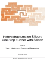
Heterostructures on Silicon: One Step Further with Silicon [PDF ebook]
Heterostructures on Silicon: One Step Further with Silicon [PDF ebook]
Придбайте цю електронну книгу та отримайте ще 1 БЕЗКОШТОВНО!
Мова Англійська ● Формат PDF ● ISBN 9789400909137 ● Редактор Y. Nissim & Emmanuel Rosencher ● Видавець Springer Netherlands ● Опубліковано 2012 ● Завантажувані 3 разів ● Валюта EUR ● Посвідчення особи 4653180 ● Захист від копіювання Adobe DRM
Потрібен читач електронних книг, що підтримує DRM
