The topic of thin films is an area of increasing importance in
materials science, electrical engineering and applied solid state
physics; with both research and industrial applications in
microelectronics, computer manufacturing, and physical devices.
Advanced, high-performance computers, high-definition TV, broadband
imaging systems, flat-panel displays, robotic systems, and medical
electronics and diagnostics are a few examples of the miniaturized
device technologies that depend on the utilization of thin film
materials.
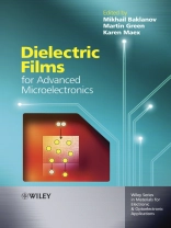
This book presents an in-depth overview of the novel
developments made by the scientific leaders in the area of modern
dielectric films for advanced microelectronic applications.
It contains clear, concise explanations of material science of
dielectric films and their problem for device operation, including
high-k, low-k, medium-k dielectric films and also specific features
and requirements for dielectric films used in the packaging
technology. A broad range of related topics are covered, from
physical principles to design, fabrication, characterization, and
applications of novel dielectric films.
表中的内容
Series Preface.
Preface. (Mikhail Baklanov, Martin Green and Karen
Maex).
1. Low and Ultralow Dielectric Constant Films Prepared
by Plasma-Enhanced Chemical Vapor Deposition. (A.
Grill).
2. Spin-On Dielectric Materials. (Geraud
Dubois, Willi Volksen and Robert D. Miller).
3.Porosity of Low Dielectric Constant Materials.
3.1 Positron Annihilation Spectroscopy. (David W.
Gidley, Hua-Gen Peng, and Richard Vallery).
3.2Structure Characterization of Nanoporous Interlevel
Dielectric Thin Films with X-ray and Neutron Radiation.
(Christopher L. Soles, Hae-Jeong Lee, Bryan D. Vogt, Eric K.
Lin, Wen-li Wu).
3.3 Ellipsometric Porosimetry. (M. R.
Baklanov).
4.Mechanical and Transport Properties of Low-k
Dielectrics. (J.L. Plawsky, R. Achanta, W. Cho, O.
Rodriguez, R. Saxena, and W.N. Gill).
5. Integration of low-k dielectric films in damascene
processes. (R.J.O.M. Hoofman, V.H. Nguyen, V. Arnal, M.
Broekaart, L.G. Gosset, W.F.A. Besling, M. Fayolle and F.
Iacopi).
6. ONO structures and oxynitrides in modern microelectronics.
Material science, characterization and application.
(Yakov Roizin and Vladimir Gritsenko).
High Dielectric constant Materials.
7. Material Engineering of High-k Gate
Dielectrics. (Akira Toriumi and Koji Kita).
8. Physical
Characterisation of ultra-thin high-k dielectric. (T.
Conard, H. Bender and W. Vandervorst).
9. Electrical Characterization of Advanced Gate
Dielectrics. (Robin Degraeve, Jurriaan Schmitz,
Luigi Pantisano, Eddy Simoen, Michel Houssa, Ben Kaezer, and
Guido Groeseneken).
Medium dielectric constant materials.
10. Integration Issues of High-k Gate Dielectrics.
(Yasuo Nara).
Dielectric films for interconnects (packaging).
11. Anisotropic Conductive Film (ACF) for Advanced
Microelectronic Interconnects. (Yi Li, C. P.
Wong).
Index.
关于作者
Karen Maex, IMEC Fellow, Silicon Process and Device
Technology Division, Leuven, Belgium & Professor at Katholieke
Universiteit Leuven
Mikhail R. Baklanov, Principal Scientist, Silicon Process
and Device Technology Division, IMEC, Leuven, Belgium
IMEC is the largest independent microelectronics R&D centre
in Europe, with over 1250 staff. R&D ranges from the design of
complex single-chip and single-package systems for
telecommunications and multimedia, new process technologies for
optoelectronics, photovoltaics, area-array packing, etc.
